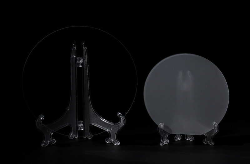
A面(11-20)蓝宝石晶片具有均匀的介电常数和高绝缘特性,因此通常用于混合微电子应用,A-plane也可用于高超导体的生长。
例如:TlBaCaCuO(TbBaCaCuO)、Tl-2212,在蓝宝石氧化铈(CeO2)复合衬底上生长异质外延超导薄膜等。
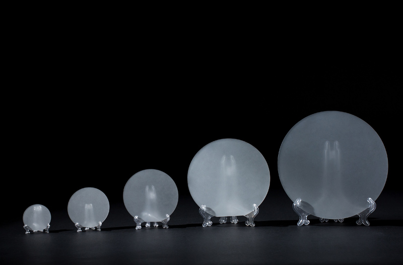
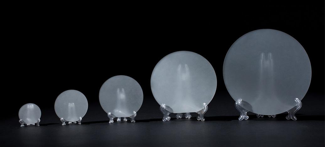
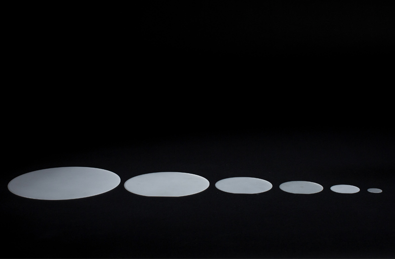
| Item | 2-inch A-plane(11-20) 430μm Sapphire Wafers | |
| Crystal Materials | 99,999%, High Purity, Monocrystalline Al2O3 | |
| Grade | Prime, Epi-Ready | |
| Surface Orientation | A-plane(11-20) | |
| Diameter | 50.8 mm +/- 0.1 mm | |
| Thickness | 430 μm +/- 25 μm | |
| Primary Flat Orientation | C-plane(0001) +/- 0.2° | |
| Primary Flat Length | 16.0 mm +/- 1.0 mm | |
| Single Side Polished | Front Surface | Epi-polished, Ra < 0.5 nm (by AFM) |
| (SSP) | Back Surface | Fine ground, Ra = 0.8 μm to 1.2 μm |
| Double Side Polished | Front Surface | Epi-polished, Ra < 0.5 nm (by AFM) |
| (DSP) | Back Surface | Epi-polished, Ra < 0.5 nm (by AFM) |
| TTV | < 10 μm | |
| BOW | < 10 μm | |
| WARP | < 10 μm | |
| Cleaning / Packaging | Class 100 cleanroom cleaning and vacuum packaging, | |
| 25 pieces in one cassette packaging or single piece packaging. | ||
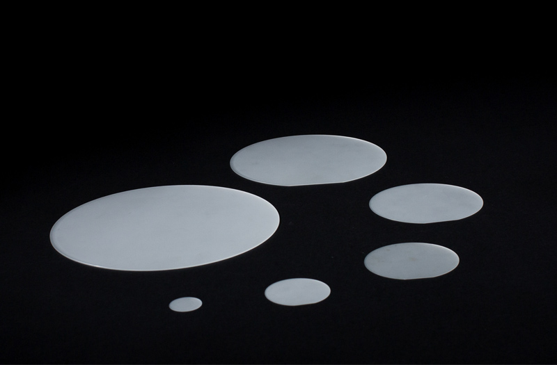
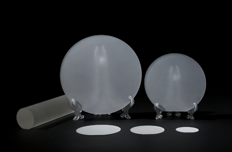
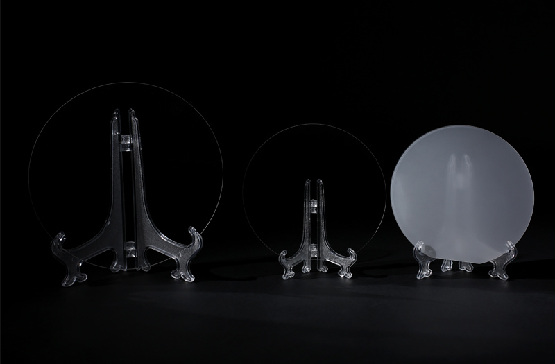
注:可依据客户需求定制的生产任意晶向、厚度的蓝宝石晶片。
 The Technical Difference Between the Kyropoulos Method and the Czochralski Method for Growing Sapphire Crystals
The Mechanism of Patterned Sapphire Substrate to Improve the Light Extraction Rate of GaN-based LED
Do You Know the Properties of Sapphire Windows?
The Technical Difference Between the Kyropoulos Method and the Czochralski Method for Growing Sapphire Crystals
The Mechanism of Patterned Sapphire Substrate to Improve the Light Extraction Rate of GaN-based LED
Do You Know the Properties of Sapphire Windows?